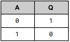
Draw a NOT gate.

Draw a truth table for a NOT gate.
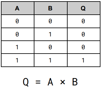
Draw an AND gate.

Draw a truth table for an AND gate.
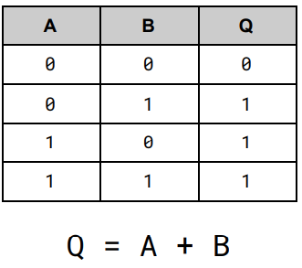
Draw an OR gate.

Draw a truth table for an OR gate.
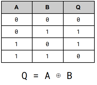
Draw an XOR gate.

Draw a truth table for an XOR gate.
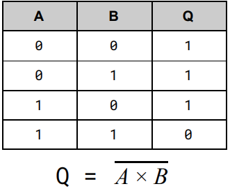
Draw a NAND gate.

Draw a truth table for a NAND gate.
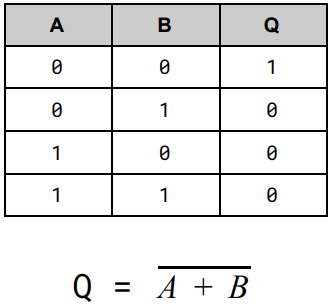
Draw a NOR gate.

Draw a truth table for a NOR gate.
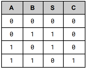
Draw the truth table for binary addition, ignoring the possibility of a carry in.
XOR gate.
AND gate.
Isolate the truth table for the SUM output.
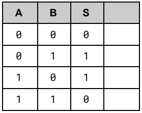
Which logic gate does this truth table resemble?
Hence SUM = A(*)BIsolate the truth table for the Carry Out Output.
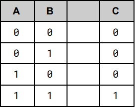
Which logic gate does this truth table resemble?
Hence Carry Out (CO) = A*BDraw the logic diagram for a half adder
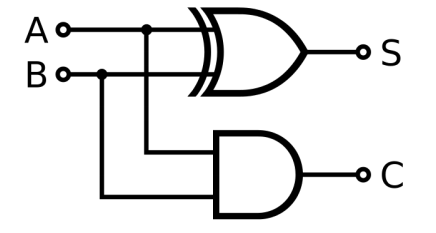
S = A ⊕ B
CO = A * B
Removing the detail of half-adders draw a simplified logic diagram of a full adder.

Describe the purpose of edge-triggered D-type flip flop.
Can store a 1 bit value, on or off.
Draw a diagram detailing the only Inputs and Outputs of a D-type flip flop.

Explain the purpose the clock signal within a D-type flip flop.
- The state of output Q can only change on the rising edge of the clock signal.
- Therefore the clock signal can synchronise many D-type flip flops to store a larger number of bits.
Where are D type flip-flops found in a computer system.
CPU registers.
Why is a NAND gate known as a universal gate.
Because all other gates can be derived from just NAND gates, so any circuit can be built using just NAND gates.